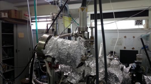
The aim of the laboratory is to investigate how physical properties arise when solid state systems shrink to the nanoscale. It is mainly devoted to atomic level controlled growth of molecular systems, low dimensional structures with desired morphology and spacing on suitable nano-structured templates. A special effort is dedicated to the growth of graphene on metallic substrates via chemical vapour deposition, graphene nanoribbons by molecular precursors, graphene nano- and micro-porous systems (see Fig. 1, right panel). Of the nanostructures grown on surfaces we study: (i) the bonding state of the elements by means of X-ray photoelectron spectroscopy (XPS), (ii) the 2D crystalline order by low-energy electron-diffraction (LEED), (iii) the control of the growth morphology by Auger electron spectroscopy (AES), and (iv) the adsorption energy by thermal desorption spectroscopy (TDS).
The XPS, LEED/AES and TDS apparatus is contained into an ultra-high-vacuum (UHV) chamber, UHV-connected to a small chamber for a fast load-lock introduction, along with several other characterisation methods and ancillary facilities for samples preparation and cleaning, atomic/molecular beam epitaxial evaporators.
Details at:

